Johns Hopkins unveils breakthrough chipmaking process for smaller, cheaper microchips

RESEARCHERS at Johns Hopkins University in the US have developed a new process to manufacture microchips that are smaller and more cost-effective than those typically used in mobile phones and cars.
Drawing on global research – including work from the Lawrence Berkeley National Laboratory in California – the team developed a metal-organic coating for microchip wafers capable of withstanding advanced lasers, enabling the creation of circuits “invisible to the naked eye”.
To create microchips, semiconducting silicon wafers are typically coated with a light-sensitive polymer known as a resist. When exposed to radiation beams, the resist undergoes a chemical reaction that allows chipmakers to etch intricate circuit patterns onto the wafer surface.
The new process developed by Johns Hopkins researchers enables circuit patterns to be created with greater precision and at sizes “smaller than the current standard size of 10nm” according to the team.
Two components
Michael Tsapatsis, Bloomberg distinguished professor of chemical and biomolecular engineering at John Hopkins, said: “Companies have their roadmaps of where they want to be in ten to 20 years and beyond. One hurdle has been finding a process for making smaller features in a production line where you irradiate materials quickly and with absolute precision to make the process economical.”
Chipmaking has already seen major advances with extreme ultraviolet lithography (EUVL), which enables patterning at scales below 10nm. Next-generation tools aim to push boundaries further, targeting features as small as 6.5–6.7nm using techniques like beyond extreme ultraviolet lithography (B-EUV).
However, B-EUV struggles to interact effectively with conventional resists. To overcome this, Tsapatsis’s team is exploring a new approach using two components: metals and an organic compound called imidazole. Their research has shown that zinc can absorb B-EUV light and release electrons, triggering a chemical reaction that imprints patterns onto imidazole.
To apply their findings to chipmaking, the researchers used a method called chemical liquid deposition (CLD) to deposit amorphous zeolitic imidazolate frameworks onto silicon wafers.
“By playing with the two components (metal and imidazole), you can change the efficiency of absorbing the light and the chemistry of the following reactions. And that opens us up to creating new metal-organic pairings,” said Tsapatsis. “The exciting thing is there are at least ten different metals that can be used for this chemistry, and hundreds of organics.”
Ongoing research
Tsapatsis and his team are currently exploring various combinations of metals and imidazoles, optimised for interaction with B-EUV radiation.
They say that this chipmaking approach “will likely be used in manufacturing in the next ten years”.
Tsapatsis said: “Because different wavelengths have different interactions with different elements, a metal that is a loser in one wavelength can be a winner with the other.”
He added: “Zinc is not very good for extreme ultraviolet radiation, but it’s one of the best for the B-EUV.”
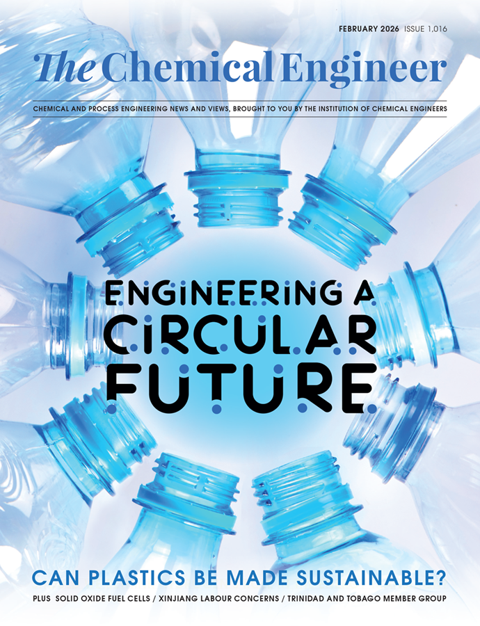
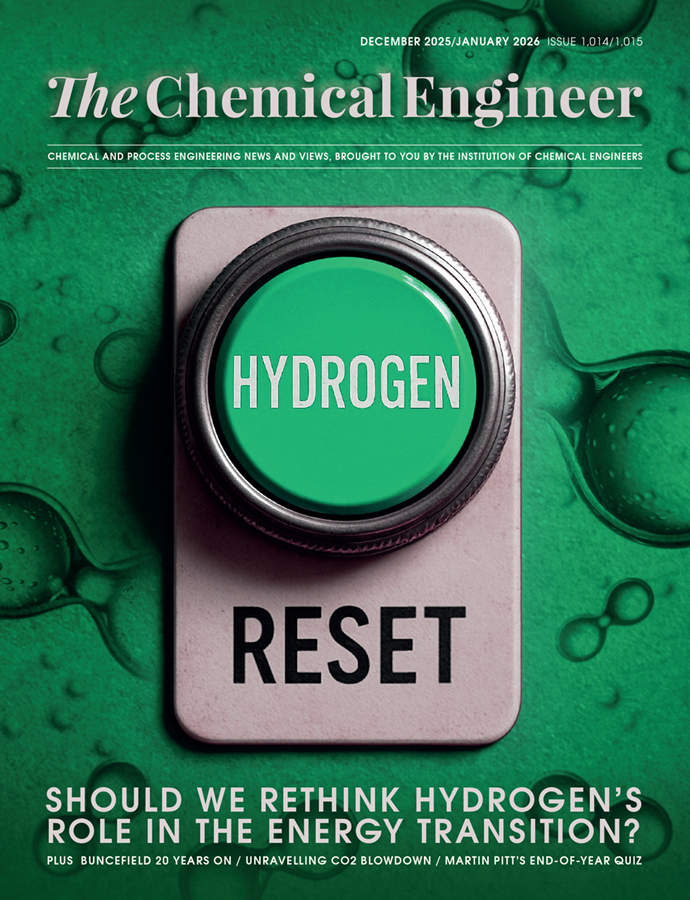
Recent Editions
Catch up on the latest news, views and jobs from The Chemical Engineer. Below are the four latest issues. View a wider selection of the archive from within the Magazine section of this site.